SEMICON Korea 2025 Highlights
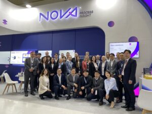
Our booth at Semicon Korea was buzzing with visitors this year. Overall, we had around 1000+ visitors and great spontaneous interactions with a curious audience.

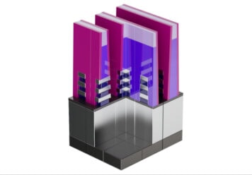
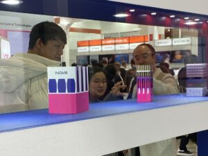
Apart for the booth design, we had a unique attraction this year, 3D printed structures of advanced semiconductor devices, demonstrating the complexity of each architecture and related challenges we’re helping our customers solve.
We also had the pleasure and honor to share our knowledge and vision at two major forums. The first was an invited talk at the MI (Metrology & Inspection) forum and the second at the CMP & Cleaning Technology session within SEMI Technology Symposium. Both received highly positive feedback, the following is a short summary of these talks.
MI Forum
The Next Wave of Convergence: Panel-Level Packaging and Co-Packaged Optics | Sang Hyun Han, VP Strategic Marketing
Sang’s presentation delved into the advancements in semiconductor device architectures driven by the AI era, focusing on the transition to 3D architectures for enhanced performance and power efficiency. It also covered the progression of system technology co-optimization (STCO) through Chiplets and wafer-level advanced packaging.
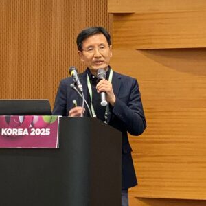
The presentation highlighted:
- Panel-Level Packaging: The industry's shift from wafer-level to panel-level packaging to reduce costs.
- Co-Packaged Optics: Discussed the integration of electronic ICs and photonic ICs into co-packaged optics using advanced packaging platforms.
- Chemical Analysis Technology: Emphasized the crucial role of chemical analysis technology in enabling the convergence of panel-level packaging with co-packaged optics.
STS - CMP & Cleaning Technology session
Cutting-Edge Integrated Metrology Solutions for Emerging CMP Challenges | Nurit Taub, Product Marketing Manager
Nurit’s presentation focused on the critical role of Chemical Mechanical Planarization (CMP) in semiconductor manufacturing, especially as the industry moves towards more complex geometries and materials. The talk emphasized the increasing demand for tighter control over wafer-to-wafer and within-wafer uniformity.
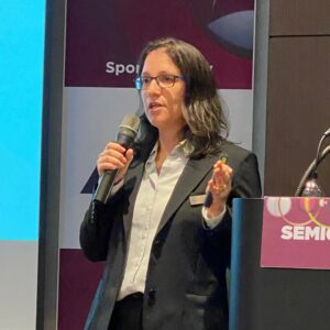
The presentation highlighted:
- Integrated Metrology (IM) as an essential for CMP process control, enabling accurate and precise measurements.
- Innovative Solutions: Discussed advanced IM solutions for increased sampling and in-die measurement, which optimize uniformity.
- Hybrid Bonding and Advanced Packaging: Explored the importance of advanced metrology in achieving peak performance and control in these areas.
- AI-Driven Techniques: Demonstrated the potential of AI in predicting process variations and improving
We look forward to SEMICON Korea 2026 and till then, our next stop is SEMICON China 2025.
See you there!