The Crucial Role of Interconnects in Semiconductor Evolution
The rapid advancement of artificial intelligence (AI), high-performance computing (HPC), and edge devices are propelling the semiconductor industry into a new era of innovation. Device architectures are evolving towards vertical scaling across logic, memory, and advanced packaging segments to meet the escalating demands for enhanced functionality and increased memory capacity. However, as chips grow more complex, efficient power delivery and robust connectivity have become critical to this type of scaling while achieving the necessary power efficiency and processing speeds for these advanced applications. Innovations such as backside power delivery networks and advanced interconnect technologies are being integrated into manufacturing processes to support this evolution. These advancements introduce new challenges, necessitating cutting-edge metrology solutions to ensure high-yield and cost-effective production of these sophisticated semiconductor devices.
Innovation in Logic Devices - Building a “real backend” through BPDN
The Backside Power Delivery Network (BPDN) is not a new concept but an innovative approach in logic device design, addressing critical power delivery and performance scaling challenges. Unlike traditional power delivery schemes, where power and signal interconnects share the front side of the wafer, BPDN moves the power delivery network to the backside of the silicon die, enabling optimized power distribution.
By dedicating the backside to power delivery, BPDN increases the density of power vias, enabling higher current-carrying capacity and better voltage regulation across the wafer. This separation also liberates the frontside interconnects for purely signal-related tasks, improving signal routing efficiency and reducing crosstalk. This approach was developed to address the challenges posed by traditional power delivery networks, which struggled with power integrity and efficiency due to increased on-chip current densities and shrinking interconnect dimensions.
The routing scheme of backside power to the front-end logic cells evolved over time to achieve a density increase at the chip level, improved power savings, and higher speed (use of higher clock frequencies). Routing schemes include Buried Power Rail, TSV Middle (TSVM), and Direct Backside Contact.
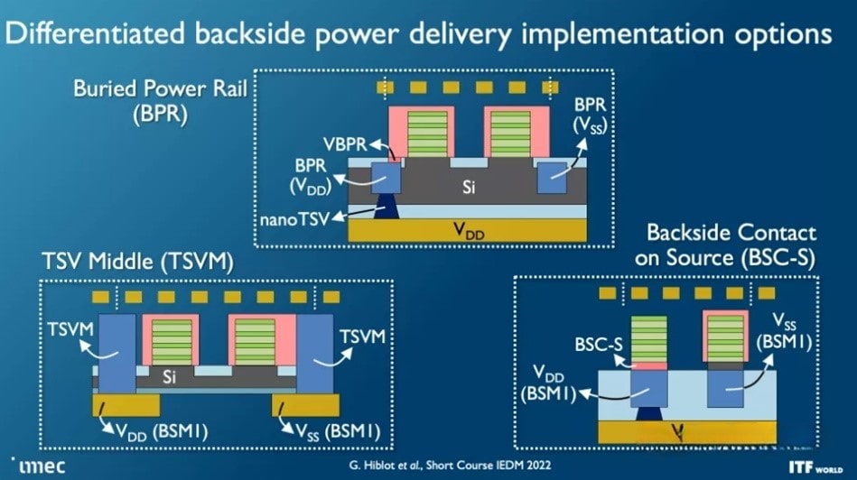
Source: imec
- Buried Power Rail (BPR) architecture – The “base” scheme where a buried power rail still connects to the transistors via a frontside metal layer, and to the power delivery network on the backside with the through silicon vias (TSV).
- TSVM (AKA PowerVia by Intel) - In this architecture, backside power is delivered to the side of the transistor contact, avoiding any power routing on the front side.
- Direct Backside Contact (DBC) - This scheme, although more complicated in fabrication, has the greatest scaling benefits of all, where contacts for power routing are formed beneath sources and drains, eliminating the through-silicon connection.
BPDNs extend Moore’s Law and also pave the way for future semiconductor architectures capable of meeting the demands of data-intensive and AI-driven applications. This holistic approach to power delivery exemplifies how process innovation can overcome critical bottlenecks in modern semiconductor devices.
Scaling DRAM Capacity and Performance – Die Stacking in HBM
High Bandwidth Memory (HBM) was created to address the increasing demands for high-speed and high-capacity memory in applications such as artificial intelligence, high-performance computing, and advanced graphics processing. Traditional DRAM architectures struggled to meet these requirements due to bandwidth, power efficiency, and latency limitations. HBM overcomes these challenges by enabling massive parallel data transfer rates, high memory density, and significantly reduced power consumption. Its architecture meets the needs of applications requiring terabytes-per-second bandwidth and the integration of ever-larger datasets.
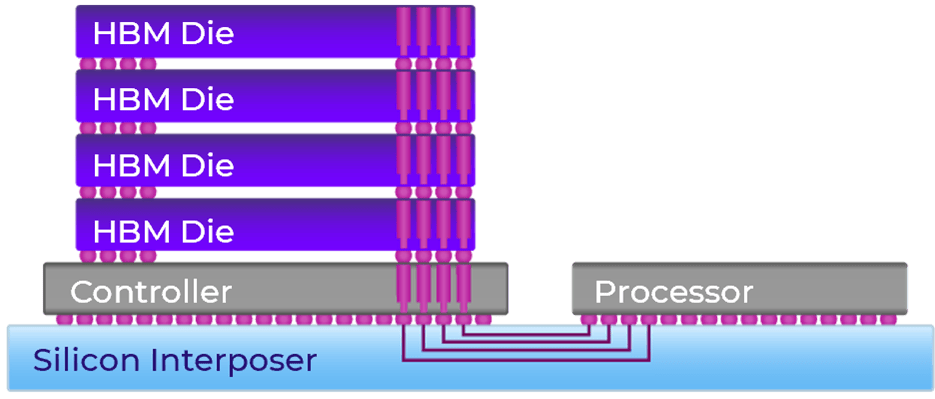
HBM achieves its performance through a vertically stacked architecture. Multiple DRAM dies are stacked using Through-Silicon Vias (TSVs), which provide high-density vertical interconnections. These stacks are connected to a base logic die through micro-bumps, ensuring a compact and efficient design. This architecture minimizes data travel distances, reducing latency and enabling higher data transfer rates than traditional memory modules.
HBM technology currently supports stacks of up to 12 DRAM dies, offering massive memory capacities suitable for cutting-edge applications. Roadmaps for future generations of HBM aim to increase the number of stacked dies and improve interconnect density, further pushing memory capacities and bandwidth. These advancements will continue to meet the evolving requirements of AI and HPC workloads while enhancing power efficiency and scalability.
Metrology plays a critical role in HBM production, ensuring the precision and reliability of its complex stacked architecture. Key challenges include inspecting TSVs for continuity, alignment, and potential defects and verifying the quality of micro-bump connections. The ultra-high-density nature of HBM interconnects demands advanced measurement tools capable of nanoscale resolution. Furthermore, ensuring uniformity across the entire stack is essential to achieving consistent electrical and thermal performance. By addressing these metrology challenges, manufacturers can optimize HBM reliability and deliver memory solutions that meet the most stringent performance requirements.
Hybrid Bonding (HB) - The Super Glue of Modern Integrated Systems
Hybrid Bonding (HB) is a transformative interconnect technology enabling direct copper-to-copper and dielectric-to-dielectric bonding at the nanoscale. This method is already employed in advanced semiconductor devices, including 3D NAND flash, high-performance logic chips, and image sensors, where its ability to achieve high interconnect density and efficiency is crucial. In the future, Hybrid Bonding is expected to drive innovations in 3D heterogeneous integration, combining multiple dies with different functionalities—such as logic, memory, and analog—into a single compact system. HB becomes an essential enabler for semiconductor architectures designed for AI, HPC, and advanced IoT applications.
At its core, Hybrid Bonding enhances interconnect density, reduces resistance and capacitance, and enables much tighter pitch scaling, often below 10 µm. These attributes significantly improve signal integrity, power efficiency, and overall performance. The process requires meticulous copper and silicon dioxide surface preparation to achieve atomic-level flatness and cleanliness, ensuring seamless electrical and mechanical connections. By eliminating traditional solder bumps, Hybrid Bonding also reduces the parasitic issues associated with conventional interconnects, further enhancing device performance. Advanced metrology tools are critical to characterize these surfaces, ensuring that bonding achieves the required precision and reliability.
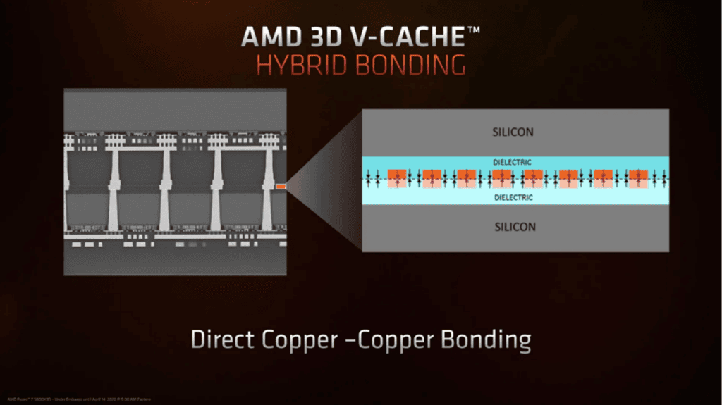
Source: AMD
Nova Prism – Addressing complex challenges in interconnects
Nova Prism®, utilizing comprehensive spectral interferometry information with advanced modeling and machine learning capabilities, is designed to address complex challenges in optical critical dimensions of interconnect technologies. One of the unique capabilities of Nova Prism® is its ability to filter out top and underlayer effects on the measurement and extract the desired POI through direct measurement. Nova Prism® supports multiple interconnect metrology applications in process control of RDL formation, TSV CMP and Hybrid Bonding.
Zoom In: TSV Metrology
As described earlier, TSV technology is used to implement backside power delivery in Logic devices (specifically buried power rails architecture), and HBM die stacking. TSVs present three significant challenges in process control. The first one is the need for high measurement sensitivity, which decreases as the aspect ratio of a TSV increases. The second is the ability to measure thick, non-periodic, isolated structures accurately, and the third is the need for complicated 3D modeling to handle complex/unknown underlayers and/or top layers in some cases. Nova Prism® overcomes all these challenges through a unique combination of its spectral interferometry (SI) technology and algorithm-assisted direct measurement that provide unparalleled accuracy and robustness.
A good example for these capabilities was demonstrated in Chiplet technology, in which comprehensive TSV characterization, including grind side measurements, is critical to ensure device reliability. The main processing steps in the TSV process flow are depicted in the illustration below. Two out of several critical parameters of interest are the depth of the TSV after the reactive ion etching (RIE) step and the reveal height of the TSV tip after wafer bonding and grind-side reveal. A robust and non-destructive measurement technique is required to access these critical parameters. Here is where SI provides a fast and reliable metrology approach to measure these two parameters in the TSV process flow while also delivering valuable information about structural asymmetry at the TSV bottom.
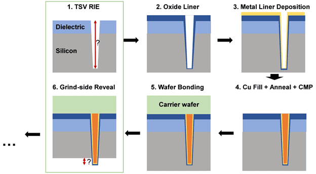
TSV process flow (main processing steps)
Read the full “Spectral Interferometry for TSV Metrology in Chiplet Technology” publication here:
https://www.novami.com/publications/spectral-interferometry-for-tsv-metrology-in-chiplet-technology/
Summary
Interconnect technologies are at the heart of the semiconductor industry evolution, enabling the performance and efficiency required by AI, HPC, and advanced edge applications. This blog explored three critical innovations driving this progress.
- Backside Power Delivery Networks (BPDNs): A groundbreaking approach in logic devices that relocates power interconnects to the backside of the silicon die. BPDNs improve power efficiency, reduce resistance and inductance losses, and free up frontside interconnects for signal routing, advancing power and performance scaling.
- High-Bandwidth Memory (HBM): Using vertically stacked DRAM with Through-Silicon Vias (TSVs), HBM achieves exceptional bandwidth, memory density, and power efficiency. These advancements are crucial for data-intensive workloads, including AI and HPC, as they support higher memory capacities and reduced latency.
- Hybrid Bonding (HB): An innovative interconnect technology that enables tighter pitch scaling, reduced parasitic phenomena, and high interconnect density. By directly bonding copper and dielectric surfaces, HB facilitates 3D heterogeneous integration, which is essential for advanced semiconductor architectures.
Advanced metrology tools, such as Nova Prism®, play a critical role in overcoming the manufacturing complexities of these interconnect technologies. By addressing challenges like TSV aspect ratios and hybrid bonding precision, these tools ensure the scalability, reliability, and performance required for next-generation devices.
These technologies collectively illustrate the semiconductor industry's commitment to innovation, enabling powerful, efficient, and compact solutions for the data-driven future.