Before studying in the US, Dr. Yi Yang had never been abroad. But she trusted her instincts, the encouragement of her family, and a chance to pursue her dreams to find success in her Ph.D. program. Today she's putting her skills in mass spectrometry to work at Nova and inspiring other young women to pursue careers in the sciences.
Yi, Tell us a little bit about yourself.
I was born and raised in Beijing and attended graduate school in the US at Stony Brook University in Long Island, New York. At Stony Brook, I earned my Ph.D. in physical chemistry. My research was focused on mass spectrometry, instrumentation, and atmospheric new particle formation. I really enjoyed mass spectrometry and instrumentation in general. That’s why when I was looking for a job, I specifically searched for those keywords, and that’s how I found Nova on LinkedIn. I then joined Nova in March 2021.
What was the subject area of your first and second degrees?
I studied chemistry in college and completed my master’s at the same university in Beijing. After that, I went to the US to complete my Ph.D.
What made you decide to move to a new country to study?
My parents encouraged me to consider studying abroad, as they didn’t have this opportunity themselves.
I was a little bit hesitant to go abroad after finishing my master’s, but they really encouraged me to. And to be honest, I miss them a lot.
Tell us a little about your experience moving to a new country and studying in a different language and culture.
Moving to the USA was a big change in my life. This was not only my first time in the USA but actually my first time abroad.
I learned a lot during this journey. I had the privilege to work on my Ph.D. in a very friendly environment. The lab team, the group I joined, and my advisor were all very welcoming. In our small research group, I was the only foreign student. All of my group members were US natives, including our host, my advisor, and my fellow students. We are still in touch to this day.
My advisor, particularly, is a good friend and someone I respect greatly. He was very helpful and shared all his knowledge to support me during my PhD studies. He encouraged me to write papers and take on professional speaking engagements. This helped me build my confidence, and eventually, I became the first Ph.D. to graduate from our group.
This positive experience is what led to me joining Nova.
What made you go into the field of chemistry?
I think I am an observant person. I tend to notice those little changes in my environment and all the details. In addition, I like doing experiments. I liked chemistry already in high school. But to be honest, before college, I was debating between chemistry and literature.
So I chose English as my double major in college. And then, I went on to earn my M.S. in chemistry.
Now that you’ve been at Nova for a year and a half, what is it that makes you choose Nova every day?
I studied mass spectrometry in graduate school and really liked it. I would like to work on mass spectrometers in my career. I choose Nova because I learn new things every day and contribute with my experience and knowledge.
Where do you see yourself in the future?
As you know, the semiconductor industry requires a lot of knowledge, skill, and experience, and I am young and still do not have much experience. In the future, my goal is one day to become an expert in the mass spectrometry instrument field.
You just recently moved to another position. What are you going to do now?
Previously I was a tech support engineer, mainly providing support wherever I was needed. In my new position, I work as a systems engineer. In this position, I define how some functions should be performed and assure the quality of each function along the way.
What kind of welcome did you receive at Nova when you joined?
The second most important reason I enjoy working every day is my colleagues. The team I’m working with are people I respect very much due to their kindness and hard work. They are incredibly friendly. These people have several decades of experience in this field and are willing to share their knowledge and support me in my everyday work.
If you had to choose one thing that characterizes you most- what would it be?
Persistence.
I always feel like I just need to keep going. Especially since completing my Ph.D., I have a deeper understanding of this because sometimes you must face and resolve the problem yourself. And you simply have to be persistent enough to solve it.
Ion implantation is a key process in the semiconductor industry but can be impacted by various factors. The article suggests using in-line Secondary Ion Mass Spectroscopy (SIMS) to improve implant process control and meet demand for consistent implantation materials by measuring peak concentration, peak depth, and dose simultaneously.
Abstract
In the semiconductor industry, ion implantation process has expanded to a wide range of applications with doses and energies spanning several orders of magnitude.
Ion implantation is a very complicated process with many parameters and factors that affect the implant profile.
For example, shadowing effects from higher aspect ratio of photoresist opening, ion channeling or de-channeling effects due to implant angle variations, and dose and implant energy accuracies are all important factors in achieving uniform device performance and good product
yield. In addition, current process controls are done on test wafers with certain time intervals, where broken sample pieces are sent outside of the fab for SIMS analysis.
The turnaround time is generally long, and the results often do not reflect the actual production conditions. It is known in some cases that, while the control charts are in good standing, the product has failed to meet its specification.
The demand for consistent implantation material is becoming more and more important. Hence, the desire for better implant process control is sorely needed.
This article explores how utilizing Secondary Ion Mass Spectroscopy, (SIMS) in-line to measure peak concentration, peak depth, and dose simultaneously to provide better implant process control.
Background and Introduction
The implantation of ions, mainly Boron, Phosphorous, and Arsenic, have a long history of use in semiconductor manufacturing. By implanting ionized atoms into a semiconductor material n-wells or p-wells can be created, changing the conductivity of the material, a technique that is often used to control threshold voltages of MOSFET devices. The creation of p-n junctions via ion implantation can prevent current flow to the substrate. Alternatively, ion implantation can create contacts to lower contact resistance and prevent diode formation. In the semiconductor industry, ion implantation process has expanded to a wide range of applications, as shown in Figure 1, with doses and energies spanning several orders of magnitude. Depending on the device, a large number of implant operations may be required in the manufacturing process flow.
Figure 1. Ion implantation applications in silicon technology at various doses and implant energies1
After implantation, the concentration distribution of the implanted ions within the material will resemble a Pearson IV distribution, with the peak depth being controlled by the implantation energy and the concentration being controlled by the implantation dose. Due to the Pearson IV distribution of the implanted ions, the only metrology method capable of measuring the peak concentration, peak depth, and dose simultaneously is Secondary Ion Mass Spectroscopy, or SIMS. By sputtering down through a material, a depth profile of the implanted atoms can be measured, giving a complete look of the shape, amplitude, and depth of the implanted ion distribution.
Figure 2 shows the distribution of implanted Boron in Silicon using a TRIM/SRIM Monte Carlo simulation.
Figure 2. Using TRIM/SRIM, (a) Monte Carlo simulation of ion implantation, and (b) Distribution of implanted Boron atoms in Silicon.
Ion Implant Metrology Challenges
Ion implantation is a very complicated process with many parameters and factors that affect the implant profile. For example, shadowing effects from higher aspect ratio of photoresist opening, ion channeling or de-channeling effects
due to implant angle variations, and dose and implant energy accuracies are all important factors in achieving uniform device performance and good product yield. In addition,current process controls are done on test wafers with certain
time intervals, where broken sample pieces are sent outside of the fab for SIMS analysis. The turnaround time is generally long, and the results often do not reflect the actual production conditions. It is known in some cases that, while the control charts are in good standing, the product has failed to meet its specification. The demand for consistent implantation material is becoming more and more important. Hence, the desire for better implant process control is sorely needed.
Metrion®
Nova’s Metrion® is a 300mm wafer-level in-line SIMS metrology system developed to seamlessly integrate with an automated high-volume manufacturing (HVM) fab environment.
It is a fully automated recipe driven metrology tool utilizing a Magnetic Sector mass analyzer to provide high quality dynamic SIMS depth profiles. It has an O2 ion source that ranges from low to medium high in beam energy for a variety of applications. Because Metrion® utilizes a low voltage secondary ion extraction field, it enables stable and repeatable measurements within a 50um x 50um metrology pad on product wafers. With multiple parallel detectors, Metrion® can measure multiple species simultaneously through the entire film stack, providing high data density capable of achieving higher depth resolution.
Process automation with built-in film analysis and recipe management make the system easy to use and shorten the time to data.
B-implant Application
Boron is one of the most commonly implanted species in semiconductors. It has one fewer valence electron than Silicon, which upon implant, results in a p-type semiconductor. As shown in Fig 1, Boron implant is used in a wide range of applications, in all types of devices in both logic and memory space.
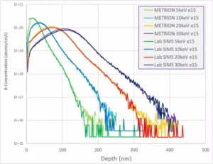
Figure 3. Metrion® vs Lab SIMS results for 1e+15 Dose B Implant in Si wafers with Implant Energies of 5, 10, 20, and 30keV.
Figure 3 compares various B-implant SIMS profiles between Metrion® and lab equipment. As can be seen, the Boron concentration vs depth profiles from Metrion® matches very well with results from lab SIMS. With a full wafer measurement capability, wafer maps can easily be generated from measurements of multiple locations on the wafers, enabling within wafer uniformity process control charts.
Figure 4 shows a wafer map example of the Boron peak concentration variation across the wafer, for the 10keV implanted B sample.
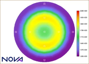
Figure 4. Wafer map of B peak concentration, 10keV Implant
As a HVM metrology tool, precision of the measurement is an important metric. In Figure 5, five profiles, which were measured at locations adjacent to each other as proxy for repeatability testing, are overlayed. As can be seen, all the profiles match very well with each other, demonstrating the stability of Metrion® SIMS measurements. For most implant dopants, a relative standard deviation (RSD) of <2% can typically be achieved.
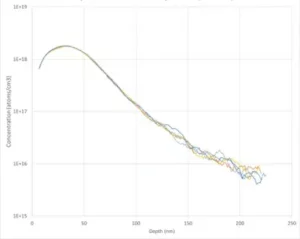
Figure 5. Overlayed of 5x repeat B-implant profiles
Summary
Nova’s Metrion® system is an innovative SIMS platform designed for the Fab environment, seamlessly integrating into an automated factory workflow. The system is engineered to deliver wafer-based high precision metrology results for process control in logic and memory devices, as demonstrated on ion implant applications. This is enabling Statistical Process Control (SPC) of the ion implant process parameters and providing in-line data correlating to electrical performance.
Authors: Benjamin Hickey, Wei Ti Li, Sarah Okada, Lawrence Rooney, Feng Zhang
First published at SIMS 23
Tell me a little about yourself.
I’m married to Peli who is a SW developer at applied materials, which means we both work in the Semi industry ????. Together we have 3 amazing girls: Yuli, Emily, and Yuval, and a Cat, Joy. I live in Beit Hashmonay and studied Management and Logistics.
What do you do at Nova and how long have you been working here?
I’ve been working for Nova for 9 years as a senior strategic buyer responsible for Electro-Optics Commodity, EFEM (FI) & Computing.
I started out as a Strategic Buyer for Computing and Electronics and over the years, my career evolved, and I became a senior buyer, and my account was focused on strategic TK. Later on, I took the role of leading the RMA cycle across the Procurement team. I really enjoy exploring the processes and optimizing them as best as possible.
From your professional experience, what makes you choose Nova every day?
I have two main reasons:
First and foremost: the people working at Nova.
I go to work every day feeling that the colleagues I work with are also my personal friends and I would almost say they are like a family.
And the second thing that makes me feel great working here is the professional challenges I am dealing with. In my position in the procurement department, Nova allows me to take responsibility for a vast array of commodities, to work with various position holders from CTO/R&D to the Production level. I’m constantly motivated to learn about new technologies, explore additional technical needs, and research so that I provide the best solutions for my counterparts at Nova.
This allows me to develop optimal procurement agreements for the organization and make the best when I manage the day-to-day activities and relationships with the suppliers to assure positive partnerships in the long run.
We all know that the procurement department has an exceptionally unique friendly atmosphere- care to share a little about this?
That is such an accurate description! The procurement team is my happy place! They are not just my colleagues or team members, they are my friends! I feel confident consulting with them and sharing my personal experiences. I know that I will always be accepted for who I am no matter what. We do have a unique team with a friendly and supportive atmosphere.
I wouldn’t exaggerate by stating that at Nova I made my closest friends. The women that I talk to on a daily basis, share professional as well as personal experiences and life events, we spend our weekends together and even traveled abroad for vacation. Even our husbands became good friends, and they have their own WhatsApp group, which is mostly used to complain about us ????
That sounds awesome.
You often travel for business- what does a typical business trip look like for you?
A typical business trip feels as though someone put my life on fast forward. There are so many things happening!
Many long-distance flights, long working days full of meetings, production reviews, and technical discussions alongside quality reviews. There is also some time for fun with dinner meetings or strolling around the cities I visit.
And then, in the morning back to the meetings. Sometimes it repeats on the following day or on my next business trip to a different location on the Globe.
One thing that always happens during these trips is that I miss my family very much. I am fortunate to have an amazingly supportive husband that helps me pursue my professional passion.
What do you enjoy doing in your spare time?
I am a huge fan of sports and in my spare time, I enjoy playing Catch ball. Basically, if I’m not at home or at work I’m on the court.
Along with my friend and colleague from the procurement department, Efrat Arad, we initiated a women’s catch ball team here at Nova. This has been a long-time dream of mine, and now, with the support of Nova’s well-being team, this is actually happening and we already have a dozen great players getting together once a week for practice. This is really a dream come true.
This is really inspiring to see how you made your dream come true.
Where do you see yourself in 5 years?
I hope to be happy and evolve my career in a way that challenges me to succeed and excel.
Let’s finalize with a question many want to ask, but never dared: What is your superpower?
I jump really really high ????
Well, that sounds very useful for someone who plays catch ball and is as ambitious and energetic as you are
Meet Shira Elnekave, an automation development specialist at Nova, a new mom – and an orthodox Jew. We sat down for a chat about her experience and insights, and how she believes more Orthodox women can find their place in today’s high-tech work environments.
Hi, Shira. Let’s start by sharing a little bit about yourself.
I’m 23 years old, married, and have a toddler son named Uriel. I’ve been working in high-tech for three years now.
I studied program engineering for two years in a seminar called “Elisheva Girls” in Jerusalem.
In my previous position, I worked as a developer. Here at Nova, I transferred to automation development, and I’ve been here since December 2021. I am an Orthodox Jew and live in a warm community of like-minded people in Rehovot.
So, what are the differences between development and automation development?
Standard development involves coding the products sold by the company. However, automation development concentrates on developing the tools or assisting programs that support the product development process.
Those tools help the developer check the code’s correctness and ensure the product is functional in all its developed versions.
We, the automation developers, are running a massive number of tests, allowing us to test our product every day, according to the updated version.
What made you decide to work at Nova?
Before coming to Nova, I worked in Tel Aviv at a company that creates personalized projects for its clients. Despite the interest and the challenge, I wanted to join a more global and stable company that would encourage personal growth. During my first interview with Nova, I was pleasantly surprised to hear, “In two years, if you’d like to change your position or evolve into a new place or study a different technology, we love that, and we are open to it.” That was one of the things that drew me in. The opportunity for personal and professional development, and of course, the fact that it is a large stable company, gave me a feeling of safety. I live in Rehovot, and Nova is also very close to home for me, especially considering that there aren’t many opportunities south of Tel Aviv.
As an Orthodox religious woman, what were the things that supported your integration process?
First of all, my colleagues’ respectful behavior was helpful. In my opinion, this comes from the top down, beginning with the management. Everyone here is encouraged to show ultimate respect and support each other’s personal and professional self-actualization.
From an aesthetic point of view, the offices are gorgeous, which has been a huge benefit for me. It’s fun to work in a beautiful environment.
And there is also my personal point of view, as an Ultra-Orthodox Jewish woman: this was part of the discussion from the start, already in the first interview. They asked me to state my needs and requirements and adjusted themselves accordingly. This was astonishing and exceeded the standards of any other company I worked for. My team manager always suggests arranging one-on-one meetings with an open door, and everyone shows respect, sensitivity, and consideration of my values and religious needs.
In my opinion, everything is well-balanced here. My values and religion take priority, and Nova ultimately respects this and supports me. I asked to be seated in a certain location, and they approved it. In addition, as a new mother, I asked to leave an hour earlier every day, and it was also approved. I feel respected and appreciated, so it is very satisfying.
How is your unique background expressed in the professional aspect?
In the professional aspect, I believe I’m not different in any way from anyone. I am doing my best to be professional, just like any other team member. Thanks to the sensitivity and care for my needs, I give 100% of myself at work with the maximum professionalism, dignity, and respect to the place that treats me in such a way.
If you’d advise your friends, colleagues, or other people to join the Nova team, what would you tell them?
First of all, I’d tell them I work here, so that’s an excellent reason for them to join (laughing). Jokes aside, I’d say to them that working at Nova gives you a sense of joy and positivity at work–which is essential, as we all know. And despite the stress and deadlines, the employee always comes first–their needs are the first priority. In my perspective, this is a distinguishing value and has led to my acceptance in the workplace.
In addition, I’d tell them about the remarkable technologies and the high level of business and tech expertise.
What are the challenges that Orthodox women are dealing with in a technological work environment? And how is it possible to deal with such challenges?
The Orthodox woman is very modest and needs to be able to set her limits when sharing a workspace with men. Communication with men at work should be mostly business related, respectful, and clear of personal talk. An Orthodox woman wouldn’t sit in a closed room with men, but here at Nova, everything is open space, so this matter isn’t an issue.
In Orthodox houses with multiple kids, there needs to be a flexible work schedule. This, too, is addressed here because at Nova, the work is hybrid and allows flexibility in the working hours, too.
In the community you’re coming from, are there some cases where you feel judged about the fact that you’re an Orthodox woman who works in the technology industry?
In my own community, as well as among the general population, the fact that I am a working Orthodox woman is completely natural. It has been quite a common phenomenon for young Orthodox girls and women to study technology and integrate in the biggest technology companies. I have friends who work at Google, Microsoft, and more. Even though in the past it was considered deviant, nowadays, it is natural and acceptable.
What do you think is the key to this massive successful integration of Orthodox women in technology work environments?
I think that what makes it possible is the will and need of Orthodox women for professional development and self-realization, along with being able to contribute financially. Also, a certain open-mindedness has been developed both within religious institutions and high-tech companies themselves. It creates opportunities to integrate different communities that were not previously included in high-tech companies.
Amazing! How do you see the future of Orthodox women in the technology market and other markets?
I believe that the future is already here. All my female colleagues from my studies are working in great companies these days, and this phenomenon is only widening and evolving. My assessment is that this will continue to trend in that same direction, and Orthodox women will be promoted to senior and key positions. They have all the qualifications and skills for that to happen.
Last question, if you’ll allow it: Would you wish for your children to also follow your same path?
Certainly. I will encourage them to do so, to take their talents and desires and invest in them. I won’t promote high-tech if it doesn’t interest them, but I’ll absolutely encourage them to pursue the professional paths they’re passionate about. However, I would be pleased if they chose high-tech because it is my domain and I love it very much.
For Rosti Talis, sports have been a lifelong passion, helping him manage his diabetes. His career at Nova has allowed him to live out his dreams of an exciting career in the sciences while balancing a career as a soccer referee.
I am 32 years old and from Ramat Gan. I recently got married in a beautiful celebration with friends and family. I have a BSc in electrical and electronics engineering from Tel Aviv University, and I am almost finished with my master’s degree. I also love sports, and exercising helps me balance my type 1 diabetes.
I have been working at Nova for about five and a half years and currently, work as a system engineering team lead as part of the Elipson project. I started at Nova in 2017 as a student in the CTO team during the first stages of the project. At the time, we could only imagine that it was possible to make RAMAN technology commercially viable–one that could work outside of the lab and create exceptional value and benefits for our customers.
What exactly do you do as part of your job?
I manage a team of system engineers, and we are expected to be experts on the Nova Elipson system. We are responsible for developing new features for the system, improving its stability, making sure it works well according to customer’s requirements and solving the challenges that the service team brings to our table. In addition, we support all the other entities that work on the product, hardware, optics, and software, as well as the service people and product managers.
When additional customer needs arise, we come up with concepts for solutions, prepare and perform feasibility analyses for them, and eventually create requirements documentation for the hardware or software teams, defining what they need to develop.
How do you manage to maintain the level of enthusiasm after being here for five and a half years?
Simply put, my work keeps me engaged and interested. Over the years, everything here has been very dynamic. The project matured and moved departments, and I matured and moved with it and eventually got promoted. This type of environment suits my personality and character. I like change, and things here change all the time—the perfect fit for me.
When I started working at Nova as a bachelor’s student in electrical engineering, I worked in the CTO team on the Nova Elipson project. It actually started as a prototype, and then we progressed to the alpha and beta stages, eventually producing it as a live commercial product.
Today we are already at an advanced stage, and the production and service teams are operating more or less independently. So, the challenges I face are constantly changing, creating the dynamic environment I enjoy.
You mentioned sports earlier. You have another line of work that is related to this, right?
That is true! Before I started working at Nova, between my military service and college, I was looking for a job, and my girlfriend (now my wife) suggested that I sign up for a basketball refereeing course. I liked the idea, but then I realized that I was more interested in soccer refereeing because it’s a sport that I live and breathe and am incredibly enthusiastic about. I completed a course, and at the beginning of my soccer-referring journey, I refereed games for young children aged 10-12. I gradually progressed to my position today as an assistant referee in the Israeli Premier League and a FIFA international assistant referee in Europe.
Since I have had diabetes since childhood, regular physical activity helps me balance my sugar levels. At every game, I have candies in my pocket in case my blood sugar levels drop.
And what are your goals for the future in this field?
I aspire to reach the top, as I’ve always aspired to reach the highest level in everything I do.
My ambition is to continue improving and working as a referee in the leading games in the Israeli Premier League and advance as far as possible in Europe.
Amazing! Do you see yourself at some point working only in this field?
No! I really enjoy this combination of the two worlds together, which are the two worlds I really like. I think the variety helps me succeed in both of them separately. Being a football referee and working as an engineer at Nova reinforce each other. At the most basic level, when I have a bad day, either at work at Nova or refereeing a bad game, I tell myself that I have the other job to cheer me up. That reminds me everything will be fine.
Being a referee also keeps me fit, which contributes to my health. On the other hand, working at Nova helps to keep my mind sharp. It allows me to constantly learn new things and evolve as a professional in the field of science, engineering, and technology, so it also keeps both my mind and body sharp.
How do you deal with having to travel a lot?
Both of my careers require travel, and this year was a little complex as I needed to travel quite a bit for Nova and for soccer.
On one occasion, I had a series of three flights to games in Europe, and then I flew to the USA on behalf of Nova. After that, I only wanted a little time to rest without traveling. But in the end, it’s an interesting experience. I get to experience new places and meet interesting people, so it is for the best. At Nova, they support my second career, so I’m able to combine both my passions.
How do your friends react to you being a soccer referee?
Everyone is very supportive and encouraging, and I really appreciate it.
Occasionally people recognize me from the stands or I get a close-up on TV during games, and then I immediately receive lots of supportive calls and messages. It’s funny because, in practice, I’m not part of the game–in my opinion, I’m a function of the game. My goal is to keep the game fair, honest, and professional.
For much of his life, Raanan Shichman struggled with a hearing disability that made communication difficult. It wasn’t until he began working at Nova and found a supportive manager and co-workers that he built up the confidence to face his disability head-on. Today, he’s thriving and encourages others to seek resources available to them.
Before I start, I want to say that even if just one person reads my story and is inspired to not to be afraid and talk about their disability, I will count that as a win. That’s part of my motivation for speaking up.
I am 42 years old and have been married for 15 years with two children, Emma and Omar. I’ve been working at Nova for a year.
I studied computer science, and I started working in technical support for MATV, an NGO, that provides nursing services for the elderly and people with disabilities. I worked there for 13 years, and there I developed empathy for the elderly and people with special needs or disabilities.
This was an experience that went beyond professional technological experience. The only thing I chose to ignore is that I, too, have special needs.
Are you willing to share a little about that?
I was born a healthy child, but at the age of two, I suffered an ear infection. During the treatment, my ear was injured, which created a reoccurring inflammation. To treat it, I had to endure eight surgeries by the age of 13. Still today I get emotional when I talk about it because it brings back a lot of feelings and memories that I tried to bury.
At 13, a miracle happened, and I was completely healthy without any inflammation or problems. Although I still had a slight hearing impairment, I was a child, and it was not tangible to me, so I felt I could manage it.
At 18, after an event in which I was exposed to loud noise, my ear infections returned, and I have been living with chronic infections ever since.
Apparently, the compounding effects of surgeries and inflammations over the years led to a decrease in hearing, and it got to the point where I was already aware of it, but I still didn’t attach importance to it and suppressed it.
I think that about five years ago, I started to feel it more. I felt that I was making a substantial effort to hear and understand and would ask people many times to repeat themselves. I was uncomfortable being in noisy environments or having conversations of more than a few sentences because it requires a lot of energy from me to concentrate and understand.
How did your environment react?
My mom kept saying she thought I should take care of it, and I was in denial. I repeatedly said that I heard perfectly well and everything was fine. I lived with a difficulty that became my reality. I didn’t see anything in it that was bad or wrong. On the other hand, I ignored that my confidence and credibility were compromised by being in the media and talking with people. I reduced the number of my work meetings because I was tired of asking again and again for others to repeat what they were saying. There were also unpleasant cases in which I did not understand what was said to me, so the answer I gave was inappropriate.
And when did you feel it was time for a change?
When I arrived at Nova, I realized that my hearing was impaired and that I needed help. And yet I was afraid to do anything about it. I was afraid and hesitant to recognize myself as a person with a disability. I was afraid of the stigma of using a hearing aid and that outsiders would label me.
Over the years, I trained myself in lip-reading skills and techniques of asking questions and checking to ensure I understood what was said. I also invested a lot of effort and energy in ensuring I understood well. The bottom line was it was good enough.
When I joined Nova, I used all these tools and techniques. Still, after a short while, I realized that all the aids I adopted were not helping me here, especially when it came to digital multi-participant conversations where there are teams from all over the world with different languages and accents. After a month of working at Nova, I realized that I was in trouble and that I was really having a hard time understanding–all because I couldn’t hear well enough.
What were you afraid would happen when you told your team and manager here about the disability?
I was new to Nova and I wanted to make the best impression at the same time, I felt that I didn’t understand the things discussed with me and that it would raise questions about my professional performance. I admit that at first, I had an irrational fear that if I share that I have a disability the people around me will not accept this.
Despite my worry and since it was vital for me to give the best of myself and to make a good impression at Nova, I finally decided to talk to my manager, and I revealed to him that I have a hearing disability and that I was going to take care of myself.
He was shocked at first but very accepting and supportive. I felt great relief when I got it out.
It turned out that after 13 years at MATAV, an organization that helps adults and people with various disabilities, in the end, joining Nova was a catalyst for treating my hearing impairment. And I must mention that my boss and all the people here are amazing and supportive; this is part of Nova’s DNA.
What significant moment do you remember in the process?
I remember several such moments.
I started the process of being fitted for hearing aids with a speech therapist and suddenly I could hear well, even sounds and vibrations I wasn’t aware of before. My wife was present with me, and at one point, she burst into tears because she realized the difference between before to now. I also realized how much I had missed avoiding dealing with my disability.
In the work environment, when I came to terms with the situation and after adjusting the hearing aids, there were a few days when I forgot them at home and felt frustrated because I realized that it would be another day with a great effort to understand. Now, I am already beyond the denial stage. I finally accept the situation and the help offered to me to live a normal life.
Even with my mother, who had supported me for all these years and encouraged me to get tested, there was a stage when I reached out to her and thanked her for her support even though, for many years, I rejected her offer to get tested.
And from all this good, one negative result came out: I lost the right to pretend I don’t hear my wife when she talks to me (laughs)!
What excites you in your daily work?
I am a people person. I have always seen myself as a conduit for connecting people and technology. At Nova, I get an opportunity daily to do just that. The desire to help and do good is an inseparable part of who I am; therefore, my profession allows me to express myself. Improving service and my desire for the employee to have the opportunity to do the job in the best way are central parts of my work.
Why do you choose to work at Nova?
I really connect with Nova’s corporate culture–the employee (the person) is at the center. I feel it in my experience as an employee and manager, as well as in interactions with my colleagues. And, of course, this people-centric culture stood out when I decided to look my disability in the eye, and I received the support of everyone around me.
In my experience, Nova sees the employee as a critical part of its existence; I feel that there is a listening ear and an understanding for the needs of the employees. On a professional level, I have room for a lot of creativity, allowing me to promote global processes regarding service improvement.
Where do you see yourself in the future?
I see myself as an integral part of Nova. My goal is that in about five years, I will be able to look back and feel that my service to Nova’s employees is excellent, and I’ve helped create tools that will enable a high level of service, so the entire team works together like a well-oiled machine.
In our companion blog post covering Metrion we explored the importance of SIMS technology for semiconductor process insight, reviewed the unique value of an automated inline tool such as Metrion, and covered the unique value Metrion offers for customers. Now let's review some widely applicable use cases.
Several use cases that we will explore for the Nova Metrion® system include contamination control, process excursion prevention, reactor matching, and uniformity control. The objectives of these use cases are to detect contaminants which can kill devices, improve barrier layer and source/drain function, maintain deposition uniformity that impacts downstream processes, and ensure wafer-to-wafer consistency.
Use Case #1: Dopant Concentration
The first use case to discuss is doping concentration for logic devices. Since very small variations in Boron concentration in a logic device wafer can impact the performance of the final logic device, Metrion can be used to qualify, monitor, and match Epi chambers in the fab to keep the production process under control.
During the Epi process, Metrion can also help control some key fabrication parameters. One of these is Epi growth uniformity, measured by tracking the Germanium concentration and the ratio of Germanium to Boron (referred to as the “Germanium fraction”).
Other key parameters the Metrion can measure include dopant concentration profile, plus peak concentration and uniformity across the wafer.
In the graph below (Figure 1) we can see an example of a single measurement of Boron, Germanium, and Silicon concentration profiles.
Figure 1 Boron Concentration Profile in SiGe
On the next graph (Figure 2 we see the tracking over time of the average Boron concentration and Germanium fraction. This data is automatically uploaded to the factory host for SPC of the Epi process.
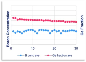
Figure 2 Automated Epitaxy SPC
As a result of chamber qualification and matching in the fab, customers can achieve tighter process control on the challenging Epi process and higher uptime of their Epi chambers.
Use Case #2: Deposition Uniformity
The second use case we will review is controlling the uniformity of Silicon-Germanium deposition in Nanosheets. Although Gate-All-Around is beginning to replace FinFET as a transistor technology because it generates better performance with lower power consumption, there are challenges to creating these nanosheets.
One of the critical steps in the manufacturing of Nanosheets or Gate-All-Around, is the deposition of SiGe.
The concentration of the Germanium, and in particular its uniform deposition on each nanosheet, dramatically affects the selectivity of the following etch process and has a direct impact on transistor performance.
In-Line Metrion SIMS can be used to monitor within-layer and within-wafer uniformity and help optimize nanosheet manufacture.
As an example, in the graph below (Figure 6), we see the Germanium concentration variation across each one of the three Nanosheets. Notice also the growth difference in the first nanosheet compared to the other two. This could mean that some of the germanium is left behind during the etch. So, monitoring the thickness of each Epi layer is key.
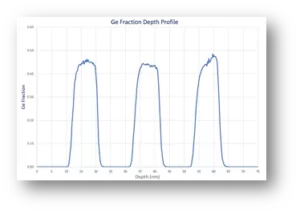
Figure 3: SiGe Growth Uniformity Monitoring
In the graph below (Figure 4) the uniformity of the Germanium concentration across the entire wafer is displayed, based on a 9-point Metrion SIMS measurement. These contour maps can be generated from as few as 5 measurement points also.
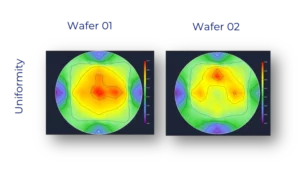
Figure 4: In-Line Germanium Deposition Uniformity Across Wafer
Use Case #3: Contamination Detection
The next use case to consider is contamination detection. There are many applications for in-line contamination control since impurities can be device killers, resulting in valuable wafers being scrapped. The sooner contamination can be detected, the more wafers will be saved, positively affecting yield and productivity for the fab.
The next example is a 3D NAND application where chlorine and fluorine concentrations were measured in the wafer stack, as shown in the graph below (Figure 5).
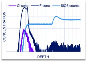
Figure 5: Cl and F Concentration-Depth Profile
Nova Metrion® generates a compositional profile through the entire wafer stack. The next graph (Figure 6) is an example of a process excursion that was identified from data uploaded to the factory host. Faster-time-to-data means that the production team can be alerted as soon as the excursion occurs, allowing process engineers to make adjustments and preserve some of the wafers — improving yield.
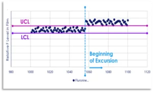
Figure 6: Fluorine SPC
Use Case #4: Implant Control
The last Nova Metrion® use case we will review is implant control for memory devices.
The uniformity and concentration of boron implants have a direct impact on device performance.
With an in-line Metrion SIMS system customers can perform weekly quals, identify process excursions, match chambers and upload uniformity maps, such as the one in the lower right-hand corner.
Gathering this data in-line takes some of the burden off the metrology labs and makes the data available for SPC via the factory host.
In the next graph (Figure 7) we see a Metrion measurement result of the concentration profile of a boron implant. This comparison between the Metrion and lab SIMS measurements shows excellent correlation.
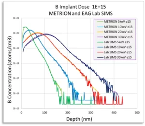
Figure 7: Boron Implant Concentration Profile
In summary, Nova Metrion® offers a variety of high-value use cases that generate faster time-to-results and reduced scrap. This saves money and improves productivity, which are invaluable to semiconductor manufacturers in today’s competitive landscape.
Nova Metrion® directly measures the composition of wafer materials using Secondary Ion Mass Spectrometry (SIMS). Metrion performs SIMS measurements in-line on full 300mm product wafers with complex film stacks for both logic and memory devices.
Performing these measurements in the semiconductor fab, rather than in a cost-and-time intensive laboratory setting, provides faster results, which reduces scrap and improves yield.
First, what is the Nova Metrion®?
The Metrion® is a SIMS tool. SIMS stands for Secondary Ion Mass Spectrometry, a technique widely used in the semiconductor industry to study material composition and depth profiling of semiconductor wafers at the atomic level. To accomplish this feat Metrion determines the concentration of various chemical species vs. distance from the surface of an IC wafer film by sputtering the surface of the wafer, capturing and analyzing the secondary ions.
Conventionally, SIMS equipment has only been available in metrology laboratories that specialize in measuring and characterizing semiconductor devices. In keeping with Nova’s ‘lab to fab’ philosophy, the Nova Metrion® has been intentionally designed to be used in-line in high-volume manufacturing (HVM).
Let’s examine the Metrion SIMS process in more detail.
Metrion SIMS uses an oxygen primary ion beam to sputter a small area on the surface of a silicon wafer. As this primary ion beam sputters through the material on the wafer film, secondary ions are ejected from the surface and are collected and analyzed by a mass spectrometer, which sorts the ions based on tiny differences in their weight. The Metrion’s mass spectrometer utilizes multiple detectors to sort the ions, and the raw data is displayed in a compositional profile showing counts of the secondary ions versus the time frame in which they are detected. Using film analysis software that is built into the Metrion process recipes, the data is quantified, converting counts into concentration and collection time into depth for each measured species.
Another key feature of Metrion is the ability to create maps of entire 300mm wafers with as few as 5 measurement points. These wafer contour maps provide a useful visual representation of within-wafer and wafer-to-wafer uniformity differences.
The numerical data from Metrion is collected and automatically uploaded to the factory host computer where it can be used by fab technical personnel to tune their semiconductor manufacturing processes through a complex mathematical technique called Statistical Process Control. This technique can generate insights that allow users to optimize costs, time, and product yield. By using Metrion as a prevention-based real-time quality control measure, fab personnel can detect trends or changes in their manufacturing process before these result in non-conforming products or scrap.
Why is semiconductor material composition so important?
As the requirements for modern electronic equipment become more complex, semiconductor chips and therefore the films built onto silicon wafers must become more complex as well. Two important types of semiconductors that vary significantly in composition and structure are logic semiconductors (used in data processing) and memory semiconductors (used in data storage). SIMS measurements performed by Metrion can help identify problems with both logic and memory production processes.
Let’s review how Metrion treats both logic and memory structures built onto wafers.
Logic structures for data processing are challenging to implement on silicon. In particular, the uniformity of the SiGe epitaxial layer is critical (epitaxy is the deposition of a thin layer of single-crystal material, in this case, a compound of silicon and germanium onto the surface of a silicon wafer). Besides SiGe epitaxy and residue control, other semiconductor composition priorities for logic chips include the precise control of dopant concentration, reactor matching, and process excursion prevention.
Semiconductor memory structures have generated significant manufacturer interest to control contamination and identify unwanted chemical residues that could reduce yield. Here, the power of SIMS to detect contamination throughout the entire device, and not just at the surface, is key. Other important SIMS functions include semiconductor material composition and thickness measurements, to improve device function.
By looking at potential diffusion, Metrion users can anticipate problems with barrier layers and source/ drain function. The deposition uniformity within wafers and from wafer to wafer is also important because this affects downstream fabrication processes. Insights in these areas provided by SIMS help to improve device performance, reduce scrap, and increase yield.
These are the main advantages of SIMS, which is used widely in metrology labs. However, lab SIMS turnaround time is too long, meaning that the data coming from the lab SIMS measurements takes too long to translate into manufacturing process control improvements, which puts many wafers at risk. Let’s look at this in more detail.
For a lab SIMS service provider, turnaround on wafer measurements can take up to two weeks. For an in-house metrology lab at a semiconductor production facility turnaround could be as short as one day, depending on the number of samples to be measured. However, time-to-results at such a producer lab could suffer if the production team required a quick result. Also, if the producer lab tool goes down, SIMS results could take months to obtain. One solution is to integrate a SIMS tool such as Metrion directly into the semiconductor production line, something it would be impossible to do with a lab tool.
What is the value of inline SIMS?
Laboratory SIMS systems only measure coupons, not full wafers. Wafers must be broken into coupons resulting in scrap. A single point is measured on each coupon. A SIMS expert is required to manually set up each measurement and to analyze the data point by point. This whole process can take days (or weeks as just discussed).
Nova Metrion®, on the other hand, measures whole wafers and is fully automated. Metrion fits seamlessly into the production line, accepting wafers from the fab’s automated transport system, loading them into the Metrion measurement chamber, measuring the wafers, providing full profile data and wafer mapping, and automatically uploading the data to the factory host. All this can be done within minutes. The real advantage of an inline Metrion SIMS system, then, is that the shorter time to data results in tighter process control and improved yield.
Figure 2 illustrates this point. In a fab with 50,000 wafer starts per month, and a turnaround time for SIMS data of 2 hours, less than 200 valuable wafers will be placed at risk. But if it takes 24 hours to get the SIMS data back from a lab, the number of wafers at risk increases dramatically to 1600. The key point here is that the faster the time to obtain results with Metrion SIMS the more wafers are saved and therefore more money is saved by improving yield.

Figure 1: Wafers at Risk by Hour for 50K Wafer Starts per Month (WSPM)
Not all the wafers have to be scrapped, so let’s imagine a scenario where there is a 3% yield loss due to some problem in the manufacturing process and, further, that this problem is identified by SIMS.
How much would a 3% increase in yield save a fab in one day? Would it save the fab $500, $5,000 or $50,000? (our assumptions are that the fab has 50,000 wafer starts per month and the cost per wafer is $1,000) The answer is that a 3% yield increase could save a fab $7,500 in a single day, a significant amount.
Now let’s imagine that a catastrophic event occurs where all of the wafers at a certain process step are lost, or if 50% of the wafers in a deposition step are lost. That’s going to have a huge financial impact.
Why can’t these savings be achieved by inline metrology today?
There are in-line solutions available, such as LEXES (Low energy Electron Induced X-ray Emission Spectrometry), Ellipsometry, 4-point probe, and XRD (X-Ray Defraction). But these techniques have to be correlated. In other words, no single metrology option exists that will provide a comprehensive picture of what is happening on the wafer.
Nova Metrion® can replace these in-line metrology options because it performs direct measurements of material composition through the entire wafer stack. Metrion also produces full wafer maps of thickness and uniformity based on several points across a wafer. Additionally, the data is automatically uploaded to the factory host for statistical process control.
What makes Nova Metrion® unique?
The Nova Metrion® includes several key features that make it well-suited for high-volume manufacturing. For example, Metrion uses an oxygen ion beam, which is fast, contamination-free, and safe for use in production.
Metrion uses multiple ion detectors, which enable multiple chemical species to be measured simultaneously. It also delivers superior depth resolution and higher data density.
Additionally, Metrion utilizes multiple modes of operation to detect a broad range of species through complex stacks, including dielectric layers.
To reduce the impacted measurement area on a wafer, Metrion utilizes a small, die-sparing raster zone, enabling SIMS measurements on product wafers without damaging valuable dies.
Lastly, the Metrion is fully automated. Offering much more than automated wafer handling Metrion has built-in film analysis recipes, recipe management, factory host communication, and compatibility with automated wafer transport.
Why is contamination from SIMS a concern?
The ultimate goal for Metrion is to measure product wafers and then feed those same wafers back into the production process, without impacting yield.
A contamination study using a Nova VeraFlex® XPS system was recently completed. The goal was to determine if Germanium ions redeposit on the surface of a wafer as a result of a SIMS measurement.
While the XPS system did pick up Germanium in the sidewall of the crater produced on the wafer surface by the SIMS primary ion beam (which is what we would expect because we’re exposing some of the SiGe layer on the edges of the crater), there was no Germanium detected in any of the other locations, including the crater center.
The conclusion from this test was that no Germanium ions were redeposited on the wafer surface during the SIMS measurement. Therefore, the Metrion did not cause any contamination and should be considered safe to use on product wafers.
What is the meaning of full automation?
Full automation means more than just wafer handling with an EFEM (Equipment Front End Module) transfer system. It includes pattern recognition to locate a specific measurement area on a pattern wafer, wafer transport, tool recipe management, and factory host communication for statistical process control. These built-in standard features enable Metrion to be used by a trained operator, rather than an experienced SIMS scientist in a laboratory setting running the film analysis on the tool.
The Nova applications team develops what are called recipes in the Metrion system. Those recipes include the film analysis and quantification, which can be set up to run automatically by the trained operator simply and quickly.
Lastly, we have automated tuning and calibration as discussed in the previous section.
All of these things equal full automation.
What is the value of full automation offered by Metrion?
It is true that fully automated systems like Metrion cost more than manual lab SIMS systems, with higher maintenance costs as well.
However, a common misconception is that capital equipment expenses and maintenance costs are the biggest drivers of ownership costs. Rather, the largest components of the entire cost to own a metrology tool like Metrion are consumables costs and uptime.
Fully automated systems have much higher availability than manual systems, usually 90% or higher. Manual systems typically have 50% or even lower availability.
And these are generous assumptions because of the manual adjustments required to set up a lab SIMS, including beam alignment, magnet settings, and switching between oxygen and cesium sources. These manual procedures, taken together with manual film analysis, can take two to four days on a lab SIMS, resulting in significant tool downtime. A fully automated system such as the Nova Metrion® has much higher availability.
We still need to factor in labor costs.
The Metrion has lower labor costs than manual laboratory systems because SIMS experts are not required to run the system. Also, the automated recipe management means that measurement jobs can be set up to run on their own. An expert operator is not needed to attend the tool 100% of the time.
The Metrion sample measurement recipes can be loaded remotely through the factory host. And the numerical data resulting from the measurements is automatically uploaded to the factory host upon completion of a job.
Compared to a manual laboratory SIMS, then, the Metrion demonstrates higher productivity.
So, what does this mean? It means that the Metrion potentially has a 20% lower cost of ownership compared to laboratory SIMS systems. With such advantages, it is clear why semiconductor fabrication facilities could benefit from Nova Metrion® SIMS.
How does Nova Metrion® achieve better depth resolution than lab SIMS and why is it important?
Now we’re going to review some of the data we have generated with the Metrion to explain its technical advantages.
Lab SIMS typically have a single detector. To collect data on multiple species during a single data acquisition run, the detectors must undergo a mass switching cycle. This means that some data will be missed because data can only be collected on one species at a time.
Metrion detectors monitor the species of interest continuously during the acquisition, resulting in higher data density and better depth resolution.
Why is a small analysis area important?
Recall that the goal for Metrion is to measure product wafers inline. For this to be viable in HVM, Metrion must be able to measure within a 50µm x 50µm2 metrology pad or scribe line. This die-sparing SIMS measurement strategy limits damage to the wafer and preserves as much of the wafer as possible so that usable die can be built on the remaining surface. Minimizing the analysis area also reduces the data acquisition time.
By comparison, the minimum measurement area for most lab SIMS is 150µm x 150µm2. Therefore, measurement runs take longer than with Metrion, data acquisition times are longer, and damage to the on-wafer die can occur. All these add to the total cost of ownership.
Summary: Why is the Metrion important?
Metrion provides wafer-level SIMS data that semiconductor manufacturers can rely on for high-volume manufacturing SPC. Metrion provides fully automated hardware and measurement sequences, with recipe-driven to support 300mm wafers. HVM worthy, Metrion provides convenient fab connectivity for SPC. Metrion offers high throughput, accuracy, and repeatability with a robust algorithm suite for material information analysis.
Metrion is only one part of Nova’s growing product portfolio. The critical metrics that all fabs must monitor include composition and thickness, homogeneity, uniformity, as well as strain, and crystallinity. Along with Metrion, Nova offers a full suite of products for materials metrology to quantify these metrics. The Nova VeraFlex® system is optimized for composition and thickness measurements, Elipson was designed to measure strain and crystallinity, and Metrion measures materials composition, uniformity, and thickness.
Creating and supporting such a complex and extensive product portfolio requires a substantial team effort. For example, the Metrion product team, comprised of scientists, engineers, production experts, and support personnel spent many hours together to make Metrion a success. And customers appreciate the effort.
In the second part of this blog post, we explore some widely applicable use cases where Metrion solved critical customer wafer fab issues successfully.
Meet Eli Meril, a Theoretical Physicist and Algorithm Developer who is part of the CTO-R&D group at Nova. He’s sharing with us more about how Nova is the perfect environment for him to nurture his love for physics while laying the foundation for groundbreaking discoveries.
Eli, since you’ve joined the Nova team, we’ve learned you’re incredibly passionate about physics. Tell us more about where that passion comes from.
I have always been fascinated by natural phenomena in the world around us, especially visual ones. I began my physics studies very informally at the age of 15, and the continuance of my education wasn’t very traditional, either. I think this is important for people to know, especially for young students who begin their academic degrees during high school (Thousands of high school students are already studying for an undergraduate degree every year). I started studying physics on my own in the tenth grade, and I immediately fell in love with it.
Wow! That’s impressive to tackle learning physics on your own at such a young age. Can you share more about your journey?
Sure. My enthusiasm for physics began after taking the Physics Olympiad test at the beginning of tenth grade. If you’ve never heard of it, I recommend looking into the International Physics Olympiad – IPhO – tests, which are super interesting. Their goal is to model natural phenomena in the various fields of physics. The questions are complex, and after a very intense year of daily studying, the eight students who make it through the strict training and achieve the highest scores are chosen for the international competition.
After a full year of self-studying, which included the major classifications of mechanics, electricity, thermodynamics, and mathematics for physicists, I ascended to an advanced stage of the Physics Olympiad tests in 2017 and began studying and training for the global competition. The level was much higher than the first-degree courses in physics. It included topics such as mechanics, electricity, electrical network, waves and optics, thermodynamics, hydrodynamics, special relativity, a little bit of statistical mechanics and Light – matter interaction, quantum mechanics, and lab work.
I’m guessing that you made the competitive team.
Yes, fortunately! When I finished training, I represented the state of Israel at the competition held in Russia in 2017. I reached 100th place in the overall competition and 6th place in Israel. We were asked about incredibly fascinating physical phenomena such as gravitational waves created by two black holes surrounding one another, superfluid vortices, and even garbage collection in space with analytical mechanics tools.
The main insight I took from the competition and can pass on to other people is to never engage in only one specific subject. The beauty of physics is that it requires knowing and combining various fields. A great example of subject combinations would be the superfluid vortices question, where the method of image charges was likened to near-wall vortices.
Great advice. Tell us a bit about your academic journey and how physics was part of that.
Shortly before the competition ended, I started my degree at Tel Aviv University. Studying for the degree was an obvious and direct continuation of the program. As soon as I began my first semester, I started working with Dr. Moshe Ben Shalom as a research assistant. Our work centered around the experimental study of two-dimensional graphene layers and various multilayered crystals (strain-wise). It was my first encounter with the experimental research world in a real lab instead of a competition. Working in a clean room is nothing like working in a lab for a test or with AFM and other microscopic methods.
An interesting thing to mention is that working on first-degree projects in research labs is a great experience that can help you understand what subjects you’re passionate about, which ways of work you connect to, whether you like the academic world or not, and more.
So, your first experience with physics in an academic setting sounds like a positive one. How did you continue to build on these interests throughout your studies?
I liked Moshe’s research and found it interesting. However, I had to leave since I was recruited to the IDF. As soon as that happened, I joined a technological unit, engaging in waves, optics, and algorithmics. We dealt with the most fascinating and essential Ground Forces projects leading the development field, and we even won the Israeli Defense prize. We worked with various industries, and the physical research was very interesting.
I continued taking classes while serving in the army. It wasn’t as fun as before, as I preferred using my time to study more physics and even teach as a private tutor and a teaching assistant. As a funny aside, once a week I used to drive to Tel Aviv University after a full day of work at the military base to teach electrical engineering students the classical mechanics course. This continued for three years. I also trained the Israeli group competing in the physics Olympic games, and I escorted our team in 2020, 2021, and 2022.
You were busy!
For sure! As I finished my military service, I continued taking university classes and teaching. I also participated in a summer project with Dr. Yoav Lahini. We studied the observation and characterization of long-lasting memory effects in mesoscopic systems, the development of an ultra-fast label free technique for tracking single viruses, and observation of topological states in disordered and quasi-periodic systems. When I finished, I started working with Dr. Naomi Oppenheimer in the hydrodynamics of high viscosities fields, searching for the solution for the first Stokes problem in its various boundaries. After experiencing and exploring multiple research fields from several directions, I realized that I find the subjects of solid-state and waves most interesting. I thus read a few optics and nonlinear optics books and watched some master-degree lessons in these subjects when I then learned about Nova.
Tell us a little bit about how you came to Nova.
While I was studying at Tel Aviv University, I received a LinkedIn message from Gilad Barak from Nova. So this is a reminder that if you’re still not on LinkedIn, you need to do it! I applied and had a job interview and fell in love with the subjects Nova’s development team is researching. I’ve now been here for about a year and a half working with the CTO physical theoretic and algorithmic group.
Can you tell us a little more about what compelled you to join the Nova team?
Sure. There are a lot of reasons, and I will tell about a small part of them. One reason I decided to work at Nova over the other industrial companies is because of the people. I liked the person who interviewed me–they’re now my boss.
Another important reason is the topics we explore here and the research Nova produces. The research my colleagues are conducting here is exciting. The physical topics of engagement we explore here are my favorite physics subjects.
We love to hear that you’ve found a career that matches your passions here at Nova. Tell us a little bit more about it.
NOVA’s CTO group conducts physical scientific studies, which are the state of the art of solid-state, optics, and nonlinear optics science. The CTO group is comprised of people holding doctorates in physics from various specialties, which enriches everyone’s knowledge. I generally think that diversity and knowledge nonuniformity may lead to discoveries and significant breakthroughs. Some examples of our team’s diverse expertise include solid-state, astrophysics, string theory, high energies, nano, and the obvious ones like optics and nonlinear optics. This diversity makes the work experience richer and more interesting; otherwise, everybody would be learning and doing the same thing.
Working in that group also resembles the academy, where there’s a purely physical problem to solve. And the process of reaching a solution might require reading scientific papers, building optic and electrooptic setups, conducting multidisciplinary research, building simulations and physical models, noise calculations, meetings and discussions with other researchers, and more. Conversations in the office corridor are always cool, and the various topics discussed always teach you a lot, in addition to the formal engagement itself.
Speaking of the academy, where do you see yourself working in the future: the academy or industry?
I still haven’t made up my mind about that. Regarding my career path, I still have a lot of time to decide. But I do believe that everyone will find their right place if they choose to do what they love the most.
It sounds like you enjoy your work, and it keeps you busy. What else do you have going on outside the office?
Apart from working, I’m also about to start studying for a master’s degree in the field of nonlinear optics with Prof. Haim Sochovsky serving as a mentor.
Do you have any parting words to share with readers?
We at NOVA are recruiting new employees for various jobs! So if you love physics, you’re more than welcome to write to me privately!
Meet Yael Kurzweil Segev, a physicist working with the New Technology group at Nova. Yael shares how her lifelong curiosity and passion for education eventually led her to Nova and how she fosters that same curious nature she’s had all her life in her own children.
Hi, Yael. It’s nice to meet you. Why don’t you start off by telling us a little bit about yourself?
I live in Mevo Horon , a beautiful settlement, with my dear family. When I have time, I like to paint and play the piano.
I Love to explore and invent since I was at a young age, and I loved physics already in high school thanks to the great teacher I had, Dr. Denino. But I never really thought I’ll have the privilege to work in physics.
I studied at the Hebrew U in Jerusalem, enrolling in an integrated science program combining physics and chemistry. There, I earned my bachelor’s and master’s degrees, as well as my Ph.D.
In the first year of my bachelor’s met my husband on campus, so the university is a very special place for my family’s story. Our first boy was born already in the last year of this degree.
My husband and I were happy to learn that all of our children love science and are curious about what their parents are doing.
I feel that Combining my family and my passion for physics is both a challenge as well as something beautiful in my life.
What drew you to study physics?
Studying physics was not in my plan at all. As I said before, even though I loved physics, I didn’t really believe that I’ll have the privilege to work in this field. I simply opened the informational resources offered by Hebrew University and saw the subjects offered there. There were a lot of interesting options, and when I saw physics, I thought, “Well, there’s another option.”
I told myself that I’d give myself a year to study physics and then would start looking for a real profession. When the year ended, I was hooked! I just couldn’t stop studying it, and somehow, I ended up with three degrees.
I really like physics, and I’m really in love with the profession.
What does applied physics mean? And how is it different from theoretical physics?
In applied physics, you also go beyond theory–you get to build the systems. It is not just theoretical calculations but rather things that are relevant and connect to existing needs and build systems. It involves a lot of lab work.
What did you do after your Ph.D.?
I’m fascinated by entrepreneurship, so it’s always been in the back of my mind. So I joined a small start-up that focused on creating affordable communication by sending mini-satellites–the size of a shoe box—into space that can make reliable internet possible in Africa.
Space is a field with many different types of technologies involved and a very strong space community, specifically among women. This enabled me to meet women from all kinds of disciplines. There was such a powerful “Girl Power” energy there, which made the experience enthusiastic, alive, and so very, very fun.
Since we are already on the subject of children, share with us the interesting educational approaches you and your husband implement at home.
We are born with natural curiosity and a lot of desire, but somewhere in life, it gets lost. I see older people who are just tired. I want to preserve that childlike sense, both for my children and for me. This is a common approach for my husband and me: we don’t let a day pass without feeling that we are doing something interesting, exciting, and promoting, both in our personal and professional lives. He’s been an engineer at Intel for 20 years and just started his master’s degree in AI. He’s the only one, a 45-year-old adult, with a bunch of young students.
I also look at the kids, and I think, “They are born with so much energy, and then you stick toys in front of them that clog their curiosity.” the fact is, we can buy the most expensive toys, and they will still end up playing with plastic water bottles.
The reason for this is that they want to handle real things. Their brain is the most flexible and develops the fastest during those stages, and it’s a shame that these energies will be wasted.
I think that if we can simplify world problems for children, they will feel significant, and their curiosity will develop to offer new ideas, maybe not revolutionary, but still interesting. They have flexible minds and are capable of creative thinking. If we are able to make them feel as if they can contribute from a young age, then they will adopt that belief throughout their life. They will realize that there is something to live for.
For example: During my tenure at Elbit, I found myself working together with my children for the simple reason that they were at home due to COVID lockdowns. At that point, I decided I did not want to work away from them, as it was a fun and enjoyable experience. I spoke with my children about my work conversations, and we discussed the ideas that came up. I even asked them to come up with their own ideas and suggestions. It created a feeling of wholesomeness, that the whole family is now recruited into my work, and for them, it was very empowering.
During the coronavirus period, one thing that was difficult for the children and my husband, and me was the loss of control and sense of ability. The fact that we discovered that there are things we can do in this new reality was most empowering and greatly helped us to get through that time. That’s basically how we managed most of the period, and very interesting things came up.
And another important thing is if I am enthusiastic about what I do, why shouldn’t they feel enthusiastic as well? If they “give in” when their mother goes to work, then they at least deserve to understand the reason for my absence. They sacrifice mommy time, my hours, for the goals I think are justified, so it’s important to me that they understand the reason behind it. Every career decision that my husband and I both make; we consult with the children because it is a joint decision. We are one organic body, heading in a single direction.
What do you do at Nova?
I belong to the New Technology group, whose goal is to explore, search for and introduce new technologies to Nova. We are examining multiple technological directions.
How does your knowledge in the world of applied physics fit into your work at Nova?
It allows me to look for solutions theoretically and then examine the solution in the lab. Now at the New Tech department, I’m able to understand technologies and systems better and estimate their ability to solve our industry’s problems. In other words, my knowledge enables me to incorporate hands-on work in the lab with conceptual physical theory. It gives me a better understanding of the systems, the needs, and the solutions.
What is the common denominator between the roles you filled?
Working with people who are enthusiastic. I admire that. Working within a group that is devoted to their position. I like the connection that’s made–a connection between technology and science of different worlds–to make them “technology, science, and people.” In other words, creating something completely new is the connector. I really adore that.
You speak with a lot of enthusiasm about your work. What is the source of your motivation? What makes you get up every morning with such enthusiasm?
It would be naive to say, “to make the world a better place.” But I grew up surrounded by an education subscribing to the philosophy that from a young age, you learn about changing the world, to contribute to the world, so that there isn’t a day or a minute that passes that goes to waste. We were given our years of life to do good, develop, and contribute during every moment.
What can you say about your work experience at Nova?
Nova is an amazing and rare combination of people who are highly professional yet incredibly humble and nice, too. I mean, the atmosphere here seems rare to me; the modesty of the people and the company atmosphere allows lots and lots of sharing and a sense of joint learning all the time, even at lunch. There are curious people here who love the science they do, and it’s a lot of fun. All of this together with everyone’s passion to create something new together leads to the success we already see and to a fulfilling and fun working environment.